


The I/O bus or expansion slots are what enables your CPU to communicate with peripheral devices. The bus and its associated expansion slots are needed because basic systems cannot possibly satisfy all the needs of all the people who buy them. The I/O bus enables you to add devices to your computer to expand its capabilities. The most basic computer components, such as sound cards and video cards, can be plugged into expansion slots; you also can plug in more specialized devices, such as network interface cards, SCSI host adapters, and others.
ISA (Industry Standard Architecture), is the bus architecture that was introduced as an 8-bit bus with the original IBM PC in 1981 and later expanded to 16 bits with the IBM PC/AT in 1984. ISA is the basis of the modern personal computer and the primary architecture used in the vast majority of PC systems on the market today. It may seem amazing that such a seemingly antiquated architecture is used in today's high-performance systems, but this is true for reasons of reliability, affordability, and compatibility, plus this old bus is still faster than many of the peripherals that we connect to it.
There are 2 versions of the ISA bus, based on the number of data bits that can be transferred on the bus at a time. The older version is an 8-bit bus; the newer version is a 16-bit bus. The original 8-bit version ran at 4.77MHz in the PC and XT. The 16-bit version used in the AT ran at 6MHz and then 8MHz. Later, the industry as a whole agreed on an 8.33MHz maximum standard speed for 8- and 16-bit versions of the ISA bus for backward compatibility. Some systems have the ability to run the ISA bus faster than this, but some adapter cards will not function properly at higher speeds. ISA data transfers require anywhere from two to eight cycles. Therefore, the theoretical maximum data rate of the ISA bus is about 8M/sec, as the following formula shows: 8MHz x 16 bits = 128Mbit/sec
The 8-Bit ISA Bus
Used in the original IBM PC computers. Virtually nonexistent in new systems today, this architecture still exists in hundreds of thousands of PC systems in the field. Physically, the 8-bit ISA expansion slot resembles the tongue-and-groove system that furniture makers once used to hold two pieces of wood together. It is specifically called a Card/Edge connector. An adapter card with 62 contacts on its bottom edge plugs into a slot on the motherboard that has 62 matching contacts. Electronically, this slot provides eight data lines and 20 addressing lines, enabling the slot to handle 1M of memory.
The 16-Bit ISA Bus
IBM threw a bombshell on the PC world when it introduced the AT with the 286 processor in 1984. This processor had a 16-bit data bus, which meant that communications between the processor and the motherboard as well as memory would now be 16 bits wide instead of only 8 bits wide.
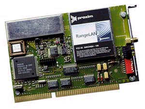
Although this processor could have been installed on a motherboard with only an 8-bit I/O bus, that would have meant a huge sacrifice in the performance of any adapter cards or other devices installed on the bus. The introduction of the 286 chip posed a problem for IBM in relation to its next generation of PCs. Should the company create a new I/O bus and associated expansion slots, or should it try to come up with a system that could support both 8- and 16-bit cards? IBM opted for the latter solution, and the PC/AT was introduced with a set of expansion slots with 16-bit extension connectors. You can plug an 8-bit card into the forward part of the slot or a 16-bit card into both parts of the slot.
The introduction of 32-bit chips meant that the ISA bus could not handle the power of another new generation of CPUs. The 386DX chips can transfer 32 bits of data at a time, but the ISA bus can handle a maximum 16 bits. Rather than extend the ISA bus again, IBM decided to build a new bus; the result was the MCA bus. MCA (Micro Channel Architecture) is completely different from the ISA bus and is better in every way. MCA runs asynchronously with the main processor, meaning that fewer possibilities exist for timing problems among adapter cards plugged into the bus.
The MCA bus also supports bus mastering. Through implementing bus mastering, the MCA bus provides significant performance improvements over the older ISA buses. (Bus mastering is also implemented in the EISA bus. In the MCA bus mastering implementation, any bus mastering devices can request unobstructed use of the bus in order to communicate with another device on the bus. The request is made through a device known as the Central Arbitration Control Point (CACP). This device arbitrates the competition for the bus, making sure all devices have access and that no single device monopolizes the bus.
Four types of slots are involved in the MCA design:
 | 16-bit
 with video extensions
| 16-bit with memory-matched extensions
| 32-bit | |
EISA ( Extended Industry Standard Architecture) was announced in September 1988 as a response to IBM's introduction of the MCA bus--more specifically, to the way that IBM wanted to handle licensing of the MCA bus. Vendors did not feel obligated to pay retroactive royalties on the ISA bus, so they turned their backs on IBM and created their own buses.
The EISA bus provides 32-bit slots for use with 386DX or higher systems. The EISA slot enables manufacturers to design adapter cards that have many of the capabilities of MCA adapters, but the bus also supports adapter cards created for the older ISA standard. EISA provides markedly faster hard drive throughput when used with devices such as SCSI bus-mastering hard drive controllers. Compared with 16-bit ISA system architecture, EISA permits greater system expansion with fewer adapter conflicts.
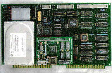
EISA was developed primarily by Compaq, and was intended as being their way of taking over future development of the PC bus away from IBM. Compaq knew that nobody would clone their bus if they were the only company that had it, so they essentially gave the design away to other leading manufacturers. They formed the EISA Committee, a non-profit organization designed specifically to control development of the EISA bus. Very few EISA adapters were ever developed. Those that were developed centered mainly around disk array controllers and server type network cards.
The VESA Local Bus was the most popular local bus design from its debut in August 1992 through 1994. It was created by the VESA committee, a non-profit organization founded by NEC to further develop video display and bus standards. In a similar fashion to how EISA evolved, NEC had done most of the work on the VL-bus (as it would be called) and, after founding the non-profit VESA committee, they turned over future development to VESA. At first, the local-bus slot seemed primarily designed to be used for video cards. Improving video performance was a top priority at NEC to help sell their high-end displays as well as their own PC systems. By 1991, video performance had become a real bottleneck in most PC systems.
The Video Electronics Standards Association (VESA) developed a standardized local-bus specification known as VESA Local Bus or simply VL-Bus. As in earlier local-bus implementations, the VL-Bus slot offers direct access to system memory at the speed of the processor itself. The VL-Bus can move data 32 bits at a time, enabling data to flow between the CPU and a compatible video subsystem or hard drive at the full 32-bit data width of the 486 chip. The maximum rated throughput of the VL-Bus is 128M to 132M/sec. In other words, local bus went a long way toward removing the major bottlenecks that existed in earlier bus configurations.
| Dependence on a 486 CPU. The VL-Bus inherently is tied to
the 486 processor bus. This bus is quite different from that used by Pentium
processors (and probably from those that will be used by future CPUs). A VL-Bus
that operates at the full- rated speed of a Pentium has not been developed,
although stopgap measures (such as stepping down speed or developing bus
bridges) are available. Unfortunately, these result in poor performance.
Some systems have been developed with both VL-Bus and PCI slots, but because
of design compromises, performance often suffers.
| Speed limitations. The VL-Bus specification provides for
speeds of up to 66MHz on the bus, but the electrical characteristics of the
VL-Bus connector limit an adapter card to no more than 40 to 50MHz. In
practice, running the VL-Bus at speeds over 33MHz causes many problems, so
33MHz has become the acceptable speed limit. Systems that use faster
processor bus speeds must buffer and step down the clock on the VL-Bus or
add wait states. Note that if the main CPU uses a clock modifier (such as
the kind that doubles clock speeds), the VL-Bus uses the unmodified CPU
clock speed as its bus speed.
| Electrical limitations. The processor bus has very tight
timing rules, which may vary from CPU to CPU. These timing rules were
designed for limited loading on the bus, meaning that the only elements
originally intended to be connected to the local bus are elements such as
the external cache and the bus controller chips. As you add more circuitry,
you increase the electrical load. If the local bus is not implemented
correctly, the additional load can lead to problems such as loss of data
integrity and timing problems between the CPU and the VL-Bus cards.
| Card limitations. Depending on the electrical loading of a
system, the number of VL-Bus cards is limited. Although the VL-Bus
specification provides for as many as three cards, this can be achieved only
at clock rates of up to 40MHz with an otherwise low system-board load. As
the system-board load increases and the clock rate increases, the number of
cards supported decreases. Only one VL-Bus card can be supported at 50MHz
with a high system-board load. In practice, these limits could not usually
be reached without problems. | |
sdf
In early 1992, Intel spearheaded the creation of another industry group. It was formed with the same goals as the VESA group in relation to the PC bus. Recognizing the need to overcome weaknesses in the ISA and EISA buses, the PCI Special Interest Group was formed.
PCI is an acronym for Peripheral Component Interconnect. The PCI bus specification, released in June 1992 and updated in April 1993, redesigned the traditional PC bus by inserting another bus between the CPU and the native I/O bus by means of bridges. Rather than tap directly into the processor bus, with its delicate electrical timing (as was done in the VL-Bus), a new set of controller chips was developed to extend the bus, as shown in Figure 5.13.
The PCI bus often is called a mezzanine bus because it adds another layer to the traditional bus configuration. PCI bypasses the standard I/O bus; it uses the system bus to increase the bus clock speed and take full advantage of the CPU's data path. Systems that integrate the PCI bus became available in mid 1993 and have since become the mainstay high-end systems.
Information is transferred across the PCI bus at 33MHz, at the full data width of the CPU. When the bus is used in conjunction with a 32-bit CPU, the bandwidth is 132M per second, as the following formula shows: 33MHz x 32 bits = 1,056Mbit/sec 1,056Mbit/sec ÷ 8 = 132M/sec When the bus is used in future 64-bit implementations, the bandwidth doubles, meaning that you can transfer data at speeds up to 264M/sec. Real-life data transfer speeds necessarily will be lower, but still much faster than anything else that is currently available. Part of the reason for this faster real-life throughput is the fact that the PCI bus can operate concurrently with the processor bus; it does not supplant it. The CPU can be processing data in an external cache while the PCI bus is busy transferring information between other parts of the system--a major design benefit of the PCI bus.
Like IEEE-1394(FIreWire), the Universal Serial Bus (USB) is a new and promising bus technology that is rapidly gaining popularity among high-end manufacturers. Essentially, USB is a cable that allows for connection of up to 127 devices through the use of daisy chaining. While it is not as fast at data transfer as FireWire, at 12M/sec it is still more than adequate for most peripherals. The USB specification was published in 1996 by a consortium comprised of representatives from Compaq, Digital, IBM, Intel, Microsoft, NEC, and Northern Telecom.
Another benefit of the USB specification is self-identifying peripherals, a feature that should greatly ease installations. This feature is fully compatible with PnP systems and provides an industry standard for future connectivity. Also, USB devices can be "hot" plugged or unplugged, meaning that you should not have to turn off your computer every time you want to connect or disconnect a peripheral. As of this writing, USB-compatible devices are still hard to find, although most newer motherboards are being made to support them. One thing to keep in mind before purchasing USB peri-pherals is that your operating system must offer USB support. Whereas the original Windows 95 upgrade and NT 4.0 do not support USB, the later OSR-2 (OEM Service Release 2) release of Windows 95 does. Future versions of Windows and NT 5.0 will fully support USB. Because the USB standard shows promise, it should become an important bus technology in the years to come.
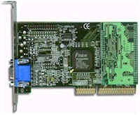
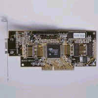
Short for Accelerated Graphics Port, a new interface specification developed by Intel. AGP is based on PCI, but is designed especially for the throughout demands of 3-D Graphics. Rather than using the PCI bus for graphics data, AGP introduces a dedicated point-to-point channel so that the graphics controller can directly access main memory. The AGP channel is 32 bits wide and runs at 66 Mhz. This translates into a total bandwidth of 266 Mbps, as opposed to the PCI bandwidth of 133 MBps. AGP also supports two optional faster modes, with throughputs of 533 MBps and 1.07 GBps. In addition, AGP allows 3-D textures to be stored in main memory rather than video memory. View PowerPoint Presentation for AGP. AGP.ppt
02/10/2001